
So I'm trying to upload a circuit board that has multiple breakaway parts since they'll always be used together. There a fab since it gives me an automated preview of my board. However, the internal cut out slots aren't showing up as cut out.
How can I guarantee that the dark purple spaces will be cut out? someone say to put "CUT OUT" in the routing spaces but I'm not sure what layer to put these on, I can't put it on the edge cuts layer.
I made the board in kicad but it's not really specific to kicad since I can't seem to find any posts that agree on how I should label the cut outs.
There are 4 individual boards to this one board.
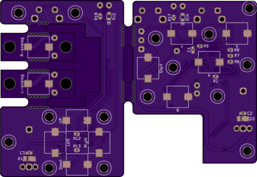
You can see the yellow edge cuts here and what the board is supposed to look like.


- Comments(1)
A****min
Aug 01.2019, 17:26:46
You could add the words CUTOUT to your two cut outs for paranoia's sake (I do). The correct layer for the cut outs and cutout text is the board outline layer.
Be aware of the minimum 100mil cutout dimension restriction. That's kinda a large and can be a pain.
The curved edges of your cutouts look good, but the finished inner sharp corners will have a radius from the round router bit.
Other board houses will have a smaller minimum slot / cutout restriction.


