Solder Mask
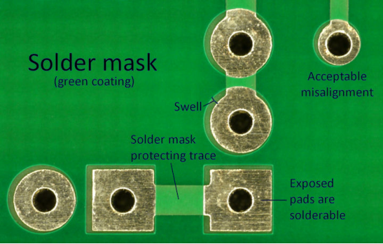
Solder mask is a protective coating for the bare board, bare boards is not only to prevent accidental solder bridging as assembly covered with mask, but also protect the board from the environment.
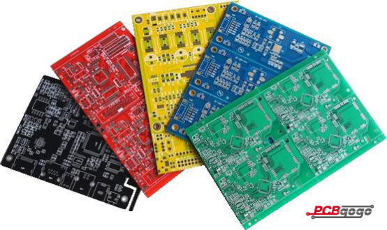
As you know, green is the most common color for solder mask, but there are many other colors available. Some colors PCBGOGO also uses:
-
Green
-
Red
-
Blue
-
Yellow
-
White
-
Black
-
Matte Green
-
Matte Black
-
Purple

Manufacturing Process for Solder Mask
A lot of people think that fabricate solder mask is not an advanced technology, and some electronic engineers can make DIY at home. However, solder mask DIY only works for simply-designed boards and it’s a little hard to make sure the products’reliability unless it’s formally applied in the final project.
When it comes to solder mask, it’s not easy for professional PCB manufacturers to fabricate solder mask. One one hand, it needs to be fully compliant with ISO 9001 quality management system, UL and RoHS certified, and committed to adhering to the strictest standards in PCB manufacturing and assembly.
One the other hand, solder mask is made up of some processes, which are satisfied with high accuracy technologies, rich manufacturing experience and up-to-date equipment.

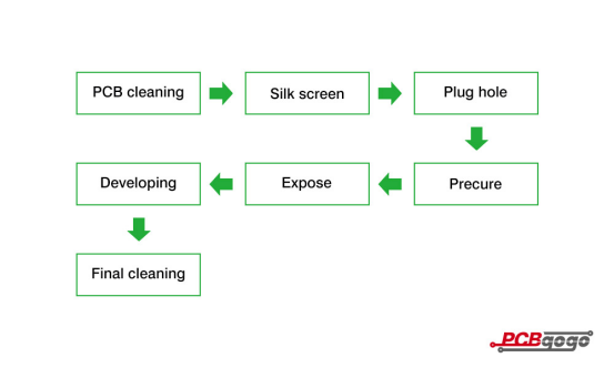
1. PCB cleaning. it’s mainly in cleaning up the oxide and dirt on the PCB surface and increasing the adhesion between anti-soldering coating.
2. Silk screen. There is mainly in silk screen as coating and you’d better plug up the hole, which controls by the adjustment of scraper.
The key points of printing process:
A: three-points bonding pressure: 6㎏/㎝2~8㎏/㎝2;
B: the scraper pressure: 4.5㎏/㎝2~6.5㎏/㎝2;
C: Scraper degree: 45°~90°;
D: printing speed: 8.5m /min~1.68m /min;
E: The thickness of ink: 15-25μm;
F: quiescence time: 15-20min;
3. Plug hole. With the development of PCB technology, more and more PCB manufacturers require that the it needs to do the plug hole with solder mask for the vias. And the plug hole is aimed at preventing anti-solder flux from the via, because it’s easy to short circuit as wave soldering.
4. Precure. It’s aimed at evaporating the solvent of ink, it’s important for the temperature, time and the control of ventilation.
5. Expose. It needs to check the PCB whether is dry or not as exposure.
6. Developing. As you know, developing is aimed at cleaning up the solder mask on the pad and do it with developing machine so as to copper foil is exposed well. The PCB should be put on the steel tower after developing.
7. Final cleaning. The boards are covered with solder mask, which need to be clean up prior to further processing such as surface finish, assembly and so on.
Solder Mask and Assembly
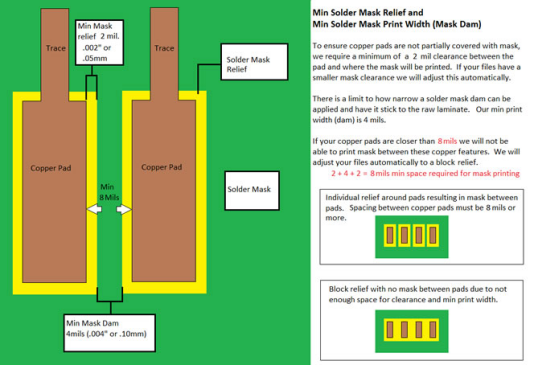
On one hand, solder mask is very important when it comes to fabricate your PCB. And the assembler will remind you that always put the solder mask dams between surface mount pads if possible, which can prevent accidental solder bridging as assembly and avoid reworking required to remove shorts.
Please pay attention to mask dam, there are limitations about minimum pad to pad spacing, in a word, not all SMD pads are having mask dams between them.Here are our minimum mask dam guidelines.

On the other hand, solder mask is also used to prevent solder starvation. For many reasons it’s easy to be solder starvation, however, the mask can prevent solder from taking away from its intended location. Open vias near the surface mount pads (such as with BGAs), can clean up the solder on the pad and open the vias without connecting. What’s more, mask is frequently used to tent or plug these vias to prevent this. You should know that cover everything with solder mask unless you need to solder to it or use it as a test point.
Please feel free to contact us if you have any questions, we will be happy to help you.
- Comments(0)
