Introduction
Prototype circuit board development is a vital phase in electronic product development. It serves as the foundation upon which the final product is made. However, the path to a successful prototype is full with challenges and pitfalls that can derail even the most meticulously planned projects.
PCBGOGO offers advanced manufacturing capabilities and expert guidance to help you avoid common pitfalls in prototype circuit board development. With their commitment to quality and streamlined processes, PCBGOGO empowers designers to bring their electronic innovations to life seamlessly.

Top Tips to Avoid Mistakes:
· Optimize Trace Geometry: Ensure proper sizing of traces for current intensity and signal frequency, using standards like IPC-2221 for guidance.
· Strategic Layout Design: Allocate sufficient space for components, considering smaller footprints and reducing inter-component distances.
· Decouple Wisely: Position decoupling capacitors close to power-hungry components to stabilize voltage and prevent oscillations.
· Pad Perfectly: Avoid landing pattern errors by meticulously sizing pads for soldering, following standards like IPC-7351B.
· Manual over Automatic Routing: Opt for manual routing to control trace placement, reducing PCB area and production costs.
· Via Caution: Use blind and buried vias judiciously to balance functionality with production costs.
· Shorten Trace Lengths: Keep high-speed signal traces short and straight to minimize signal degradation and electromagnetic interference.
· Tackle EMI: Group elements by functionality and minimize right angles in traces to mitigate electromagnetic interference.
· Antenna Accuracy: Optimize antenna layout for wireless communication, ensuring impedance matching and signal transfer efficiency.
· Regular Reviews: Conduct regular design reviews to identify and rectify errors early in the development process.
There are some of the common pitfalls encountered in PCB prototype development and strategies are provided to avoid them.
Insufficient Planning and Design Verification
One of the primary causes of PCB prototype failures is inadequate planning and design verification. Rushing into the development process without a clear understanding of the project requirements, component selection, and layout can lead to costly mistakes down the line.
To mitigate this risk, it's essential to invest sufficient time in the planning and design phase. This includes conducting thorough research, defining clear objectives, and performing comprehensive design verification tests using simulation tools before moving to fabrication.
Poor Component Selection and Sourcing
Choosing the wrong components or relying on unreliable suppliers can spell disaster for your PCB prototype. Common issues include:
· component shortages
· counterfeit parts
· Compatibility issues.
To mitigate these risks, it's crucial to carefully select reputable component suppliers and verify the authenticity of the components. Additionally, opting for readily available and well-documented components can streamline component sourcing process and reduce the likelihood of delays.
Inadequate Thermal Management
Heat dissipation is a critical consideration in PCB design, especially for high-power applications or densely populated boards. Failure to address thermal management concerns can result:
· Performance degradation
· Premature component failure
· Safety hazards.

To avoid these issues, incorporate proper thermal design techniques such as heat sinks, thermal vias, and proper airflow within the enclosure. Thermal simulation tools can be used to identify and address hotspots early in the design phase.
Neglecting Signal Integrity
Signal integrity issues can wreak havoc on the performance of your PCB prototype, leading to data corruption, timing errors, and electromagnetic interference (EMI). Common culprits include:
· improper trace routing
· impedance mismatches
· inadequate ground planes
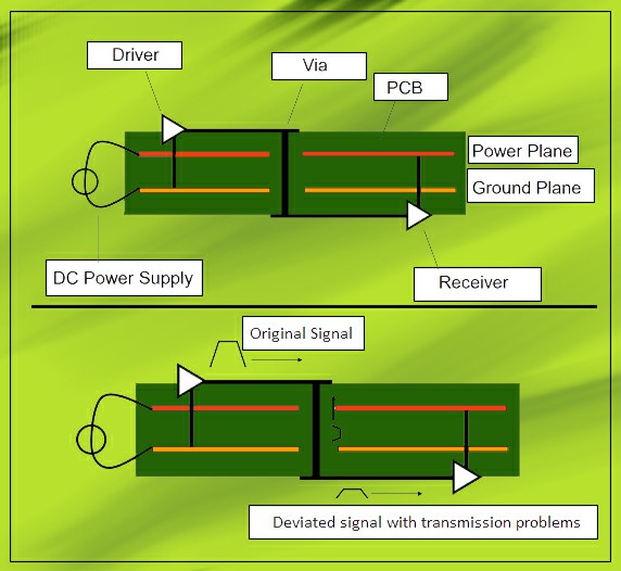
To maintain signal integrity, adhere to best practices for high-speed design, such as maintaining consistent trace widths, minimizing signal reflections, and implementing differential pairs for critical signals. Additionally, perform signal integrity analysis using simulation tools to identify and rectify potential issues before fabrication.
Lack of Design for Manufacturability (DFM) Considerations
Designing a prototype that is not optimized for manufacturing can result in costly rework and production delays during the transition to mass production. Factors such as component placement, solder mask clearance, and penalization should be carefully considered to ensure seamless manufacturing.
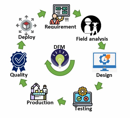
To mitigate this risk, involve manufacturing partners early in the design process and incorporate DFM guidelines into your PCB layout. Additionally, leverage advanced PCB design software that provides DFM checks and feedback to identify potential manufacturing issues upfront.
Failure to Test and Iterate
Lastly, neglecting to thorough PCB testing and iterate on your PCB prototype can lead to overlooked design flaws and performance limitations. Rigorous testing, including functional testing, environmental testing, and reliability testing, is essential to validate the design and identify areas for improvement.
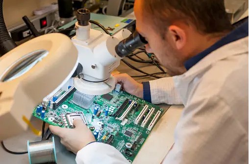
Be prepared to iterate on the design based on test results and feedback from stakeholders. Continuous refinement and optimization are key to achieving a successful prototype that meets the desired specifications and performance targets.
Conclusion
Navigating the complex landscape of prototype circuit board development requires careful planning, meticulous attention to detail, and a proactive approach to risk management. By avoiding common pitfalls such as insufficient planning, poor component selection, thermal management issues, signal integrity concerns, neglecting DFM considerations, and inadequate testing, you can increase the likelihood of success and accelerate the path to market for your electronic products. Remember, investing time and resources upfront to address these challenges will ultimately pay dividends in the form of a robust and reliable PCB prototype.

- Comments(19)
s****sss
Apr 30.2024, 15:59:43
**
Apr 30.2024, 02:16:25
T****son
Apr 05.2024, 04:05:39
g****mza
Mar 22.2024, 01:15:41
g****mza
Mar 22.2024, 01:15:06
s****sss
Mar 21.2024, 17:12:38
T****son
Mar 17.2024, 15:44:09
J****eld
Mar 14.2024, 12:01:22
[link name=google]https://google.com/[/link]
[google->https://google.com]
((https://google.com/))
((https://google.com/ google))
[https://google.com/ google]
[[https://google.com/ google]]
[L=google]https://google.com/[/L]
"google":https://google.com/
J****eld
Mar 14.2024, 12:01:11
J****ock
Mar 11.2024, 14:35:44
T****son
Mar 07.2024, 18:18:33
S****ham
Mar 07.2024, 15:31:15
S****ham
Mar 07.2024, 15:30:03
S****ham
Mar 07.2024, 15:29:06
m****ass
Mar 06.2024, 23:03:10
**
Mar 03.2024, 19:31:13
Navigating Chernobyl tours on this service's website сhernobylstory.com is like embarking on a virtual exploration of one of the world's most intriguing destinations. The site provides an array of meticulously crafted itineraries, each offering a unique perspective on the Chernobyl Exclusion Zone. With detailed descriptions, captivating visuals, and transparent safety guidelines, travelers can confidently plan their visit to this historical site. It's the go-to platform for those seeking an immersive and educational journey into Chernobyl's past.
R****yan
Mar 01.2024, 05:27:23
I****ive
Feb 29.2024, 09:40:13


